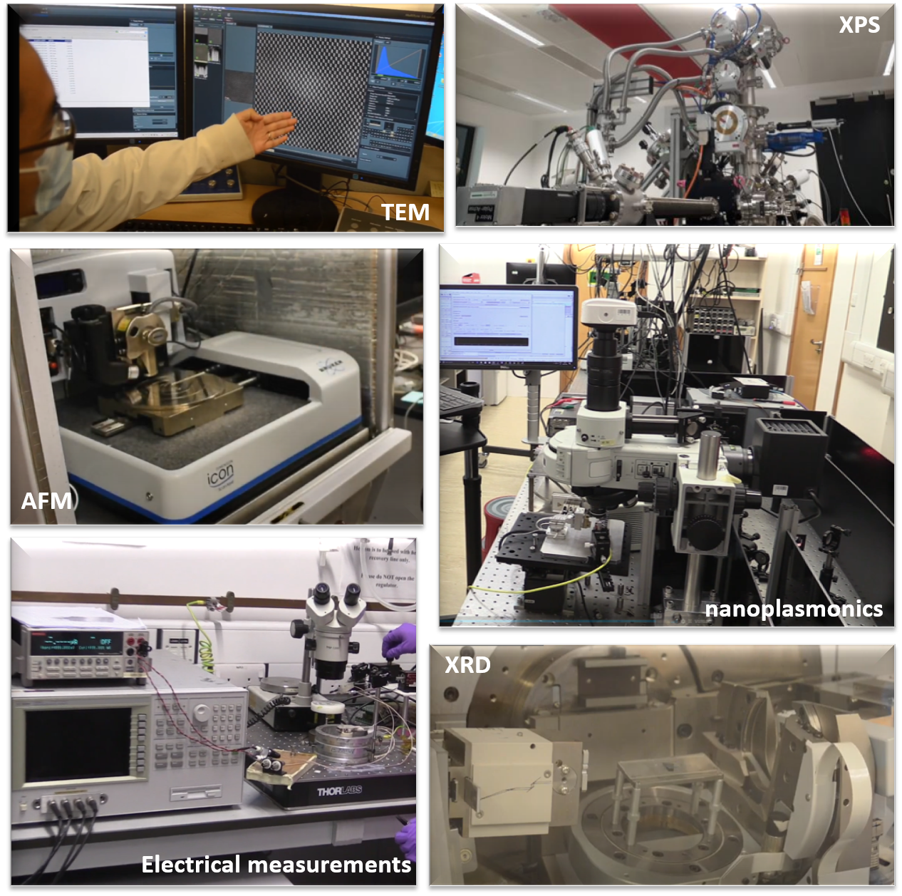
Our team has a wide range of expertise in thin film growth, materials characterisation, and devices fabrication/testing.
| Growth Capabilities | Electrical characterization | Spectroscopy | Surface imaging | Microscopy | Device Fabrication |
| PLD, Sputtering, ALD | DC, RF, ferroelectric testing, impedance measurements | Nanoplasmonic optical spectroscopy, environemntal XPS, in-situ XPS, synhcrotron based XAFS | AFM, CAFM, PFM | STEM, nano-focused X-ray imaging (diffraction, XAFS) | Sputtering, evaporation, lithorgraphy |
Growth
Pulsed Laser Deposition, among other growth techniques is performed in the Driscoll and Wang group labs.
Materials Characterisation
Various materials characteristion techniques are utulised within our team. Including:
X-ray Photoelectron Specroscopy (XPS) - in ultra high vacuum or near-ambient pressure for in-situ XPS
High resolution X-ray diffraction (HRXRD) and synchrotron-based diffraction/spectrocospy
Atomic Force Microscopy (AFM) and Conductive AFM
Scanning Transmission Electron Microscopy (STEM), Energy-dispersive electron specroscopy (EDS)
Nanoplasmonic optical specroscopy
Device Fabrication and Testing
Resistive switching devices are fabricated in our team usin sputtering, evaporation, and photo/e-beam lithography.
Electrical characterisation is performed for device testing incuding: DC, RF, and ferroelectric testing, as well as thin film impedance measurements, and piezo force microscopy (PFM)


